The accelerator package is where the rack computes: GPU or custom-accelerator dies sit beside stacks of high-bandwidth memory on a silicon interposer, mounted on a large organic substrate. Each Blackwell GPU packs 208 billion transistors on two reticle-limited dies joined at 10 TB/s, and a GB300 NVL72 rack carries 20 TB of HBM3E across its 72 GPUs (NVIDIA).
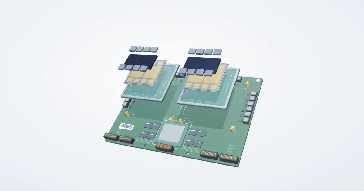
A superchip-style module: two GPU packages and a host CPU on one board. Each GPU package places two large logic dies and eight HBM stacks on an interposer, mounted on an organic substrate that fans the connections out to the board.
The logic dies do the math, the HBM stacks feed them data, the interposer wires dies and memory together at very fine pitch, and the substrate and module board carry power in and signals out.
Illustrative gpu module example. Designs differ by manufacturer; the model is not a bill of materials.
What to look for: The two large dies at the centre of each package, the eight memory towers around them, the thin interposer beneath, and the much larger substrate and board below.
Three companies: SK hynix, Micron and Samsung, all named as memory suppliers in NVIDIA’s FY2026 10-K. Micron says its HBM3E is designed into GB300 NVL72 and the AMD MI350 Series; SK hynix reports HBM4 mass shipments since Q2 2026; Samsung says its HBM4 is designed for NVIDIA Vera Rubin. Samsung’s HBM3E qualification for NVIDIA is reported, not confirmed, and none of the three discloses its share of a given GPU.
Is a packaging or substrate company a GPU supplier?
Not in the sense of designing the chip. TSMC fabricates the dies and joins them to HBM on an interposer (CoWoS), and Amkor and ASE’s SPIL are NVIDIA’s named packaging and test partners in Arizona. Substrate makers such as Ibiden and Samsung Electro-Mechanics build the organic base the package sits on, using Ajinomoto’s ABF film. Their filings describe AI demand but name no GPU customer, so their exposure is to AI packaging in general, not to one rack.
NVIDIA and AMD design the GPUs, while Broadcom, Marvell, Alchip and GUC design custom accelerators for cloud customers. TSMC makes the Blackwell dies and packages them with CoWoS, with Amkor and ASE named as packaging partners; SK hynix, Micron and Samsung make the HBM, and Ibiden, Samsung Electro-Mechanics and Unimicron make substrates built on Ajinomoto’s ABF film.
Open each company below for its source and limitations. Sector membership does not establish a confirmed supply contract.
Inside the assembly
GPU compute dies
Two reticle-sized logic dies joined into one GPU, built on a leading-edge foundry process. They run the matrix math of training and inference. Custom accelerators designed by or for cloud companies are the main alternative.
Stock-link scope: The compute dies. NVIDIA designs Blackwell and Blackwell Ultra (208 billion transistors on two reticle-limited dies, custom TSMC 4NP) and AMD designs the Instinct MI350 and MI455X; NVIDIA discloses that TSMC fabricates Blackwell. Custom accelerators are the alternative: Broadcom co-develops OpenAI-designed accelerators and racks (its other XPU customers are unnamed), Marvell develops custom AI silicon for unnamed customers, and the design-service houses Alchip (an N3 accelerator for a North American cloud provider, from May 2026) and GUC (AI accelerator design support) disclose programs without naming customers. Intel’s Gaudi 3 is a merchant AI accelerator with no documented rack-scale deployment. Hyperscaler chip designers (Google TPU, AWS Trainium) are not mapped because they do not sell the chips as components. Samsung is named as an NVIDIA wafer foundry but not for Blackwell GPU dies, so it is not mapped here.
Towers of 8 to 12 DRAM dies joined by through-silicon vias and placed beside the logic dies. Eight stacks give one GPU hundreds of gigabytes and several terabytes per second of memory bandwidth.
Stock-link scope: Three companies make HBM, and NVIDIA’s FY2026 10-K names all three (SK Hynix, Micron, Samsung) as memory suppliers. Micron is mapped first because its release names GB300 NVL72 and GB200 NVL72 (and the AMD MI350 Series) for its HBM3E. SK hynix reports HBM4 mass shipments from Q2 2026 and a 56.4% HBM revenue share in Q1 2026 (its prospectus), without naming customers. Samsung says its HBM4 is designed for NVIDIA Vera Rubin and in mass production; its HBM3E qualification for NVIDIA (Sept 2025) is reported only. No source gives a supplier’s share of a specific GPU.
A silicon interposer, or silicon bridges in an organic layer, carries thousands of fine wires between the logic dies and the HBM. Building it and assembling the dies onto it is the advanced-packaging step.
Stock-link scope: TSMC’s CoWoS is the packaging NVIDIA names in its 10-K; TSMC produces 5.5-reticle CoWoS and plans 14-reticle packages with 20 HBM stacks for 2028. NVIDIA named Amkor and ASE’s subsidiary SPIL as its packaging and testing partners in Arizona (Apr 2025), and both describe 2.5D silicon-interposer packages for GPUs and HBM in their annual filings. Which steps each performs for a given GPU (chip-on-wafer or on-substrate) is not disclosed, and that Blackwell uses the CoWoS-L variant is reported, not confirmed in our sources. Intel’s EMIB-class packaging has no documented AI-rack program here and is not mapped.
Also in this part (not publicly listed):Siliconware Precision Industries (SPIL) Subsidiary of ASE Technology Holding (3711.TW)
ABF package substrate
A large multilayer organic substrate made with build-up film. It fans the interposer’s dense connections out to the pitch of the board and carries power to the dies.
Stock-link scope: ABF (FCBGA) package substrates. Ibiden (strong GPU demand, substrates for AI servers and switching ICs) and Samsung Electro-Mechanics (FCBGAs for AI accelerators and server CPUs) disclose AI-accelerator substrate supply without naming customers. Unimicron markets FCBGA for AI servers and switches, and Nan Ya PCB is developing large, high-layer substrates for AI and HPC (positioning). Kinsus is named by ASE as an IC substrate supplier, with no AI program documented. Ajinomoto supplies the ABF insulating film to substrate makers and is an upstream enabler, not a substrate maker. Which substrate maker supplies a given GPU is reported, not disclosed.
The board that carries two GPU packages and one CPU with their power stages and high-speed connectors. It docks into the compute tray and its cold plates.
Stock-link scope: The superchip board carrying two GPU packages and one Grace CPU is an NVIDIA design (GB300 Grace Blackwell Ultra Superchip). Wistron builds GB300 superchip boards and AI servers in Texas (NVIDIA partner documents). Victory Giant makes the printed circuit boards for AI computing cards and GPU baseboards (its investor record, July 1, 2026), but no source names the fabricator of a specific rack-scale module board. NVIDIA’s 10-K names Hon Hai among contract manufacturers without saying which builds the module, so Hon Hai is listed under Builders, not here; Fabrinet’s disclosed role is optical. The module’s power stages sit under voltage regulators.
Disclosed: AMD’s Advancing AI 2026 release describes Helios with 72 MI455X GPUs, 18 Venice CPUs and Pensando networking, and names its adopters and system partners.
Disclosed: Alchip’s Q2 2026 investor presentation reports N3 accelerator shipments to a North American cloud service provider from May 2026; the customer is not named.
Partner-disclosed: NVIDIA names Amkor for packaging and testing in Arizona, and Amkor’s 2025 10-K describes 2.5D interposer packages for HBM and graphics processors.
Partner-disclosed: NVIDIA names SPIL for packaging and testing in Arizona, and ASE’s 2025 Form 20-F describes its 2.5D silicon-interposer packages for GPUs and AI accelerators.
Disclosed: GUC’s 2025 annual report describes its support for customers’ AI accelerator chips, and its Q2 2026 release attributes most 3 nm turnkey revenue to cloud projects.
Partner-disclosed: NVIDIA’s DGX B300 page names the Intel Xeon 6776P host CPU, and NVIDIA’s Sept 2025 release describes the custom x86 CPU collaboration.
Disclosed: Marvell’s FY2026 10-K describes its custom AI silicon, electro-optics DSPs, AEC DSPs for AI scale-up and scale-out, PCIe retimers and Teralynx switches.
Disclosed: Micron’s GTC 2025 release names GB300 NVL72 and GB200 NVL72 for its HBM3E, SOCAMM and SSDs, and its June 2025 release names the AMD MI350 Series.
Disclosed: NVIDIA’s GB300 NVL72 and DGX GB300 pages give the GPU, CPU, NVLink, ConnectX-8, BlueField-3 and NVLink Switch counts, and its FY2026 10-K names its foundry, memory and assembly partners.
Disclosed: Samsung Electro-Mechanics’ Q2 2026 results cite FCBGAs for AI accelerators and server CPUs and MLCCs for AI servers; customers are not named.
Disclosed: Samsung’s GTC 2026 release says its HBM4 is designed for NVIDIA Vera Rubin and in mass production; its Q2 2026 results report scaled-up HBM4 sales.
Disclosed: SK hynix’s Q2 2026 results report HBM4 mass shipments and SOCAMM2 growth; NVIDIA’s FY2026 10-K separately names SK Hynix as a memory supplier.
Partner-disclosed: NVIDIA’s Blackwell page and FY2026 10-K name TSMC’s 4NP process and CoWoS packaging; TSMC’s own release describes its CoWoS roadmap.
Disclosed: Victory Giant’s July 1, 2026 investor-relations record describes its leading share in AI computing-card, UBB and switch boards; its 2025 annual report gives the results.
Disclosed: upstream enabler; Ajinomoto’s ASV Report 2026 describes ABF as a material for package substrates, with demand driven by AI, data centers and networks.
Evidence groupings are not investment ratings. Companies may appear in multiple sectors.
Also in this sector (not publicly listed)
Siliconware Precision Industries (SPIL) Subsidiary of ASE Technology Holding (3711.TW)
Named by NVIDIA, with Amkor, as a packaging and testing partner in Arizona (Apr 2025). SPIL is a wholly owned subsidiary of ASE Technology Holding, whose row (3711.TW) covers it.