How this system works
A flip-chip quantum processor: a qubit die bump-bonded face down onto a wiring die, wire-bonded into a gold-plated copper package with microwave launches, and closed inside magnetic shielding under the mixing-chamber plate.
Qubits are superconducting circuits on a chip. Josephson junctions make them behave like artificial atoms, a low-loss substrate keeps their energy from leaking away, bump bonds bring wiring to the middle of the chip, and the package and shields keep it cold, connected and quiet.
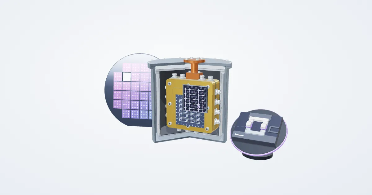
What to look for: The qubit die on its wiring die, drawn circuit side out so the lattice shows (in a flip-chip it faces down), the grid of indium bumps, the magnified SQUID and its two junctions, the wafer the dies are cut from, the gold package with its launches, and the cut-away shield cans around it.
Compare the right roles
Who makes quantum processor chips?
Mostly the quantum-computer makers themselves. IBM makes its wafers at a 300 mm facility in Albany, Google built Willow in its own Santa Barbara fab, Rigetti runs Fab-1 and sells Novera QPUs to others, and IQM produces chips in its own clean room. Foundries are emerging: SkyWater, owned by IonQ since July 31, 2026, makes D-Wave’s wafers; GlobalFoundries launched a quantum foundry business in May 2026; and STMicroelectronics fabricates Quobly’s silicon spin-qubit devices. None of them reports chip revenue separately.
Do large materials and equipment companies supply qubit chips?
Only a few document it, and none reports quantum sales separately. Applied Materials works with Qolab on materials and wafer-level fabrication for superconducting qubits, Oxford Instruments markets deposition of superconducting films and junction barriers, and Veeco sells ALD and MBE systems for quantum research. For substrates, Soitec makes silicon-28 FD-SOI wafers for Quobly, Silex is commissioning a silicon-28 plant for Silicon Quantum Computing, a QuTech qubit recipe names wafers from GlobalWafers’ Topsil, and Kyocera researches sapphire substrates. Most of these are research or prototype links rather than disclosed volume supply.
IBM, Google, Rigetti and IQM design and fabricate their own superconducting qubit chips, Fujitsu co-develops them with RIKEN, and D-Wave’s wafers come from SkyWater, part of IonQ since July 2026, while GlobalFoundries and STMicroelectronics are building quantum foundry roles. Applied Materials, Oxford Instruments and Veeco bring deposition and etch tools, and Soitec and Silex run dedicated silicon-28 programs for spin qubits. The specialist evaporator, e-beam and magnetic-shield makers named in qubit recipes (Plassys, Raith, Amuneal) are private.
Open each company below for its source and limitations. Sector membership does not establish a confirmed supply contract.
Inside the assembly
Qubit chip
A silicon die patterned with about a hundred superconducting transmon qubits, the tunable couplers between them and a readout resonator for each. The quantum state lives in these circuits.
Stock-link scope: The qubit die. Makers that design and fabricate their own superconducting chips come first: IBM (Nighthawk links 120 qubits with 218 tunable couplers; wafers made at a 300 mm facility in Albany, where its company Anderon runs a pure-play quantum wafer foundry), Google (105-qubit Willow from its Santa Barbara fab), Rigetti (Fab-1, chiplet-based Cepheus systems, Novera QPUs sold to others), IQM (chips from its own clean room), D-Wave (superconducting annealing QPUs whose wafers SkyWater makes), AWS (the Ocelot cat-qubit prototype) and Fujitsu (a 256-qubit chip co-developed with RIKEN). IonQ is mapped only because it has owned SkyWater, D-Wave’s wafer foundry, since July 31, 2026. GlobalFoundries (a quantum foundry business launched in May 2026 with photonic, ion-trap and spin-qubit partners, developing superconducting processes) and STMicroelectronics (Quobly’s silicon spin-qubit devices in Crolles) are foundries, and Intel’s 12-qubit Tunnel Falls is a silicon spin chip. Trapped-ion, neutral-atom and photonic machines use different hardware and sit under makers. QuantWare, Oxford Quantum Circuits, Quobly and Qolab are private; research fabs such as imec and MIT Lincoln Laboratory are not companies and are not mapped.
Also in this part (not publicly listed): SkyWater Technology Subsidiary of IonQ (IONQ), Anderon Subsidiary of IBM (IBM), QuantWare Not publicly listed, Oxford Quantum Circuits Not publicly listed, Quobly Not publicly listed, Qolab Not publicly listed
Josephson junctions & films
Aluminium–aluminium-oxide–aluminium tunnel junctions, the nonlinear element that makes each circuit a qubit, and the niobium, tantalum or aluminium films of its wiring. Deposition and lithography tools and high-purity target metals make them.
Stock-link scope: The Al/AlOx/Al tunnel junctions and the Nb, Ta or Al films are made inside the qubit makers’ own fabs, so the listed exposure is to tools and process know-how. Oxford Instruments markets plasma tools for quantum devices, including atomic-layer deposition of NbN and TiN films and of Al2O3, AlN or TaN tunnel barriers for Josephson junctions (positioning); Applied Materials is named by Qolab (for superconducting qubits) and by HPE for materials engineering and wafer-level fabrication; and Veeco’s 10-K lists quantum computing among the uses of its ALD and MBE systems. Published qubit recipes name private tools: Plassys electron-beam evaporators and Raith e-beam writers. Sputter-target and metal makers (Materion, JX Advanced Metals) and JEOL’s e-beam writers have no documented qubit role in the sources captured and are not mapped.
Also in this part (not publicly listed): Plassys Not publicly listed, Raith Not publicly listed
Substrate wafers
High-resistivity silicon or sapphire wafers, chosen because they absorb very little microwave energy. Isotopically purified silicon is the substrate of choice for spin qubits.
Stock-link scope: Superconducting qubits are built on high-resistivity silicon or sapphire, and silicon spin qubits need isotopically purified silicon-28. Soitec supplied the first custom 28Si FD-SOI wafers for Quobly, cycling in STMicroelectronics’ 300 mm fab since December 2025, and Silex finished building a laser plant for enriched silicon-28 in June 2026 (commissioning due late 2026) with Silicon Quantum Computing as initial offtake partner. For superconducting chips, QuTech’s 2026 flip-chip qubits started from >20 kΩ·cm wafers ‘sourced from Topsil’, a GlobalWafers company, and Kyocera researchers published superconducting vias through sapphire substrates for quantum circuits (2024); both are thinner, research-level links. Quobly also names Air Liquide and the unlisted Orano as silicon-28 partners without detailing their roles, so Air Liquide is not mapped here. The largest wafer makers (Shin-Etsu, SUMCO, Siltronic) document no qubit role and are not mapped.
Also in this part (not publicly listed): Orano Not publicly listed, Topsil GlobalWafers A/S Subsidiary of GlobalWafers (6488.TWO)
Flip-chip bonds
Indium bumps that join the qubit die face down onto a second die carrying readout and control wiring, so signals reach the middle of the chip from above instead of only from its edges.
Stock-link scope: Flip-chip bonds and 3D integration. Rigetti’s 10-K describes in-house superconducting multi-chip bonding for chip-level 3D integration and superconducting through-silicon vias, used in its chiplet-based systems, and AWS’s Ocelot stacks two bonded silicon chips of about 1 cm² each. GlobalFoundries says it is developing a cryogenic and superconducting heterogeneous interconnect platform (positioning), and Oxford Instruments markets deep silicon etch for through-silicon vias in quantum circuits; its PECVD tool appears in QuTech’s 2026 indium-bump qubit recipe. The indium in that recipe came from Indium Corporation and the gold evaporator from AJA International, both private, and QuantWare (private) sells VIO chiplet packaging. No bonder maker (Besi, Kulicke & Soffa) documents a quantum role, so none is mapped.
Also in this part (not publicly listed): Indium Corporation Not publicly listed, AJA International Not publicly listed, QuantWare Not publicly listed
Sample package
A gold-plated copper enclosure holding the chip, a circuit board, wire bonds and microwave launches. It thermalizes the chip at the mixing chamber and connects it to the coaxial lines.
Stock-link scope: The gold-plated copper sample package with its PCB, wire bonds and microwave launches is usually designed in house by qubit makers. Fujitsu is mapped because its release with RIKEN shows the 256-qubit chip in a sample package built for their 3D connection structure (Apr 2025). QuantWare (private) sells packaged QPUs and VIO packaging services. No listed maker of qubit sample packages is documented in the sources captured; generic machining, plating and PCB suppliers are not mapped, and Kyocera’s documented quantum work concerns sapphire substrates, not packages.
Also in this part (not publicly listed): QuantWare Not publicly listed
Magnetic shielding
Nested cans of high-permeability alloy and superconducting metal, sealed against infrared light, that keep stray magnetic fields and radiation away from the qubits.
Stock-link scope: Nested high-permeability and superconducting cans around the package. The documented suppliers are private specialists: Amuneal builds cryogenic magnetic shields for cryostats, SQUIDs and SRF cavities, and Magnetic Shields Ltd markets shielding for quantum computing; QuTech’s 2026 test setup used a copper can and two mu-metal shields. Carpenter Technology’s HyMu 80 nickel-iron alloy is sold for magnetic shielding in general, but no source ties it or another listed alloy maker to qubit shields, so the part has no listed supplier.
No verified direct company match in the current universe.
Also in this part (not publicly listed): Amuneal Not publicly listed, Magnetic Shields Ltd Not publicly listed